background image background image background image

Electronic Packaging Days 2025

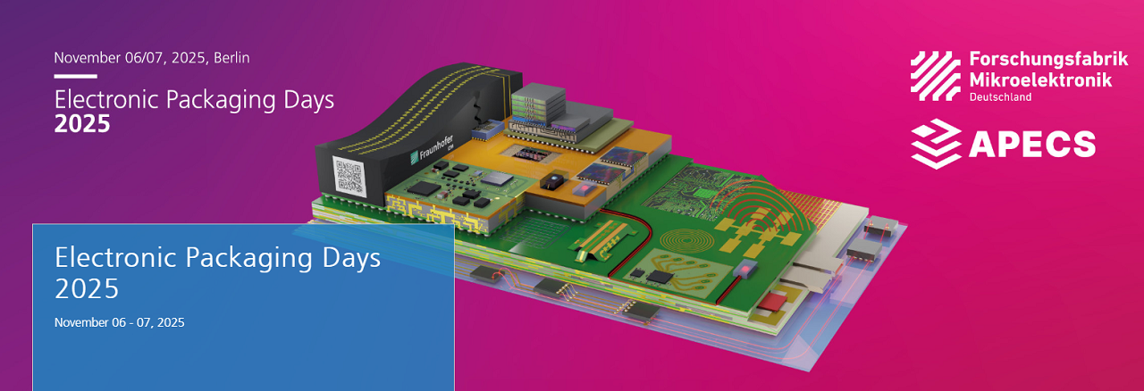
On 6 and 7 November, Fraunhofer IZM invites customers and partners from industry to Berlin for the “Electronic Packaging Days”. This event is designed to facilitate direct interaction between IZM researchers and companies. The aim is to present current research and technological developments in microelectronic packaging and heterogeneous system integration, and to discuss these with partners. During coffee and lunch breaks, participants can choose from a variety of options – 12 IZM laboratories and the clean room will be open for half-hour tours. Expert sessions will also offer the opportunity to discuss the institute's technological services with IZM experts and find out more about the APECS pilot line.

Nov 6, 2025 11:00 - 22:15 - Nov 7, 2025 08:30 - 15:30
Fraunhofer Institute for Reliability and Microintegration IZM

Gustav-Meyer-Allee 25
Building 17/3
13355 Berlin Germany

Program

Details on the event and registration can be found on the event website.

  • 11:00 – 11:30 Coffee & Welcome
  • 11:30 – 12:00 Keynote: Packaging is Shaping Future Electronics | Prof. Ulrike Ganesh
  • 12:00 – 13:00 Session: 1.1: The APECS Pilot Line | Session Chair: Rolf Aschenbrenner
    Keynote: Enabling the Future – APECS Pilot Line | Rolf Aschenbrenner
    Navigating the Future: Innovation and Roadmapping in Wafer Level Packaging | Dr. Manuela Junghähnel
    Next-Level Panel Level Packaging | Ruben Kahle
    How to Use the Pilot Line – Strategic Partnerships and Service Offer | Erik Jung
    13:00 – 14:00 Lunch
  • 14:00 – 15:00 Session: 1.2: Chiplet – Driving Force for High Performance Computing | Session Chair: Dr. Michael Schiffer
    Keynote: Function-Driven Innovation: How Technology Follows the Needs of Chiplet Systems | Dr. Michael Schiffer
    Size Does Matter: How HPC Module Form factors Increase with Chiplet Technology | Dr. Ole Hölck
    High-Speed Design, Fabrication and Assembly of Interposers on System Boards for Chiplets and HPC | Dr. Alexander Gäbler
    High-End Performance Packaging – Latest Trends | Markus Wöhrmann
  • 15:00 – 17:00 Coffee Break – Networking – Expert Sessions – Lab Tours
  • 17:00 – 18:15 Session: 1.3: Sustainable Electronics | Session Chair: Dr. Nils F. Nissen
    Keynote: Why the IT Giants Are on the Quest for Enhanced Environmental Transparency | Karsten Schischke
    Going Green Combines Environmental, Reliability and Business Aspects | Dr. Nils F. Nissen
    Green Deal for Microelectronics – Material & Energy Efficiency by Design | Carsten Brockmann
    Presentation of the IZM Researcher Award 2025: Energy and Carbon Footprint of Advanced Computer Hardware for HPC and AI Systems | Dr. Lutz Stobbe
  • 18:15 – 22:15 Get-together
  • 08:30 – 9:00 Coffee & Welcome
  • 09:00 – 10:00 Session: 2.1: Future Compute I | Session Chair: Dr. Tanja Braun & Dr. Michael Schiffer
    Keynote: Material Trends in High-End Performance Packaging | Prof. Martin Schneider-Ramelow
    Photonics for AI Data Centers Dr. Tolga Tekin
    Photonic Glass Core Substrates for Data Centers and Optical Computing | Julian Schwietering
  • 10:00 – 10:45 Session: 2.2: Future Compute II | Session Chair: Dr. Tanja Braun
    Keynote: Tailoring Packaging for Advanced Quantum Applications | Dr. Hermann Oppermann
    Soft Medical-Grade Substrates for Neural Interfaces | Prof. Vasiliki Giagka
    Packaging Technology in the Digital Realm: Digital Twins & AI-related Tools | Karl-Friedrich Becker
  • 10:45 – 11:45 Coffee Break – Networking – Expert Sessions – Lab Tours
  • 11:45 – 12:30 Session: 2.3: Power Electronics | Session Chair: Dr. Andreas Middendorf
    Keynote: Power Electronics – Strategies for a Cost-Effective Production | Prof. Eckart Hoene
    Molded Packages for Power Devices – Technologies and Specifications | Tina Thomas
    Challenges of Reliable Power Electronics | Dr. Stefan Wagner
  • 12:30 – 14:30 Lunch Break – Networking – Expert Sessions – Lab Tours
  • 14:30 – 15:15 Session: 2.4: RF System Integration meets Leading Edge Packaging | Session Chair: Harald Pötter
    Keynote: RF Packaging Architectures and Design for Communication, Sensing, Computing and AI Applications | Prof. Ivan Ndip
    Application-Specific Design and Packaging of Radar Modules and Systems | Dr. Christian Tschoban
    Design for Reliability of Advanced Packages for 5G and 6G Wireless Infrastructure | Dr. Johannes Jaeschke
  • 15:15 – 15:30 Recap & Farewell Prof. Ulrike Ganesh and Prof. Martin Schneider-Ramelow
  • Cleanroom
  • Material Characterization | Corrosion Lab
  • System Integration & Interconnection Technologies
  • Condition Monitoring (ECM Lab)
  • Analytics (FIB, REM & XPS | ESCA)
  • EBSD & Moisture Lab APECS Pilot line
  • Assembly & Encapsulation Lab
  • Substrate Line
  • Electronic Textile Lab
  • Photonic Lab
  • Power Lab
  • Functional Testing of Compact Radar Modules
  • Energy Efficiency and Functional Testing
  • RF for Material, Interconnect and Antenna Testing
  • Next-Generation 3D Heterointegration at 300mm (digital)

Expert Sessions:

  • Wafer Level System Integration
  • System Integration & Interconnection Technologies
  • Environmental & Reliability Technologies
  • RF & Smart Sensor Systems
  • APECS Pilot line

You will be asked to register for individual guided tours and expert sessions when you register.